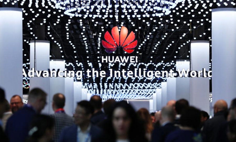
Huawei’s New Chip Architecture Opens a Path Beyond U.S. Technology Controls
 Facebook
 Twitter
 Linkedin
 Google +
Three different organizations, three different domains, the same underlying instinct: don’t wait for the conventional path to open up, build a completely different one.
For 60 years, the chip industry has operated on a single guiding principle: make transistors smaller, and everything gets faster. It’s called Moore’s Law, and it has delivered every generation of computing most of us have ever known. It’s also running out of road, physically, economically, and technically.
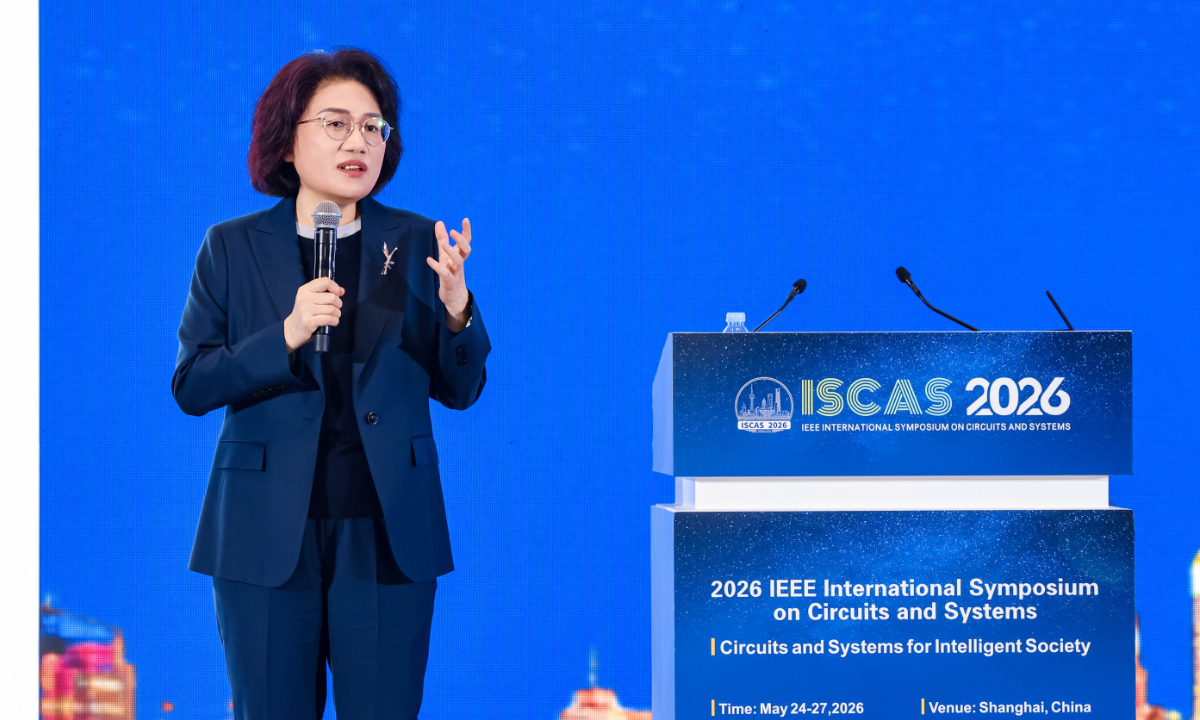
On May 25, at an international semiconductor conference in Shanghai, Huawei proposed what it believes comes next.
Moore’s Law has a problem, and Huawei has a proposal
The challenge with Moore’s Law lies in its practical application. Making transistors smaller requires increasingly advanced manufacturing equipment, and that equipment is becoming harder to build, more expensive to operate, and available to fewer and fewer companies. For Huawei specifically, access to the most advanced manufacturing tools has been banned since 2022 through U.S. export controls.
But China has long been building toward semiconductor self-reliance as a national strategic goal, and Huawei’s latest announcement indicates that this is part of a longer mission, not simply a response to external pressure, but the result of years of deliberate internal development and key technology breakthrough.
He Tingbo, President of Huawei’s semiconductor business, presented the company’s Tau Scaling Law at the IEEE International Symposium on Circuits and Systems in Shanghai. Instead of asking how small a transistor can be made, Huawei is asking how fast information can move through a chip. The emphasis shifts to signal propagation time, tau, and compressing it at every level of the chip’s architecture. The result is better performance without needing smaller transistors.
The pragmatic implementation of this idea is an architecture Huawei calls LogicFolding. The simplest way to think about it: traditional chips are built flat, like a single-story building. LogicFolding stacks the circuits vertically, like adding floors. More floors mean more processing power without shrinking anything.
Huawei says this approach already delivers 55 percent higher transistor density and 41 percent better power efficiency than conventional chip designs. The company has spent the past couple of years mass-producing 381 chips built this way across a range of products. The first flagship Kirin chip, Huawei’s line of processors used in its smartphones and devices, is set to fully adopt LogicFolding and ship this fall.
Looking further ahead, Huawei projects that by 2031, its high-end chips will match the transistor density of a 1.4-nanometer process. For context, that’s the level TSMC, the world’s most advanced chipmaker, is currently targeting for 2028. The gap, in other words, is now measured in years, not decades.
A new pattern of Chinese innovation
It’s worth understanding where the industry currently stands. Several analysts have recognized that the concepts beneath LogicFolding, advanced packaging, and 3D chip stacking are not entirely new. TSMC, Samsung, and Nvidia have all invested in similar approaches. Nvidia CEO Jensen Huang has pointed out that stacking technologies have been in the industry for nearly a decade.
However, what makes Huawei’s announcement noteworthy is that it tries to overcome production challenges. Designing and mass-producing chips using these methods, with a largely domestic supply chain, is a meaningfully different engineering challenge. Huawei’s announcement is an attempt to clear that bar. Rather than relying solely on ever-smaller process nodes to deliver performance gains, it’s focusing on architectural innovation, advanced packaging, and system-level optimization. Whether all of its performance targets are achieved remains to be seen, but the significance lies in its effort to create a new pathway under existing constraints.
We can see the same innovation patterns in other fields. In early 2025, researchers at Peking University announced a 2D transistor built from new materials that operates 40 percent faster than TSMC’s 3-nanometer devices while consuming 10 percent less energy. Then came DeepSeek, which matched frontier AI performance not by accessing better hardware, but by redesigning how models are trained, dramatically cutting compute requirements. Now, Huawei is proposing a new scaling law for the chip industry itself.
Three different organizations, three different domains, the same underlying instinct: don’t wait for the conventional path to open up, build a completely different one.
The announcement has immediate effects on China’s AI industry. Huawei’s Ascend chip series already sits at the center of China’s domestic AI computing stack, powering models including DeepSeek’s latest. If LogicFolding delivers on its performance claims as it rolls out across the Ascend line through 2027 and 2028, the gap between Chinese AI hardware and Nvidia’s best-in-class hardware will close considerably. That matters for every Chinese company and research institution currently working with hardware restrictions for AI.
The future of AI chips in China
This doesn’t mean the semiconductor gap has closed. Global leaders still hold advantages in design and manufacturing experience, production scale, software ecosystems, and supply chain depth. Huawei’s fall Kirin launch will be the first real commercial test of whether LogicFolding performs is as claimed, and that question can only be truly answered and the LogicFolding be proved over time.
But the more major shift may already be underway. China’s semiconductor ambitions are nothing new. What Huawei showed in Shanghai on May 25 is that those ambitions are producing concrete, technically specific results, a new architecture, already in mass production, with a product on the shelf before the end of the year. Whether or not LogicFolding changes the industry on its own, it is a clear sign that China is not standing still while it builds. It is evolving on its own terms, innovating at its own pace, and building toward a future that no longer depends on American technology.